High-Speed Interface and EDA Laboratory
Establishment and Key Technical Indicators
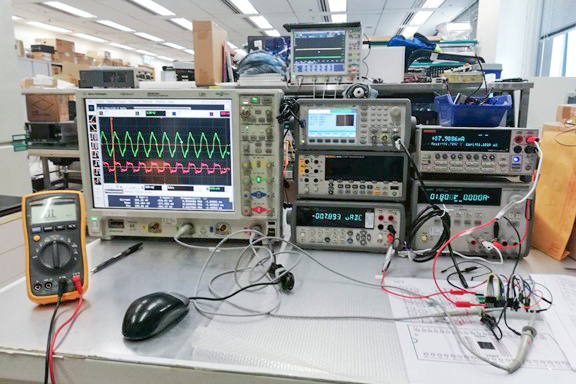
The High-Speed Interface and EDA Laboratory is facilitated with the Thermo Fisher’s transmission line pulse (TLP) test equipment with a pulse width of 100ns and a rise time of 10ns. It meets the requirements of the general on-wafer ESD characterization of ESD devices. The Laboratory is also equipped with the Barth’s VFTLP (Barth 4012) imported from US with a pulse width of 10ns and a rise time of 1ns which meets the CDM pulse on-wafer characterization. In addition, the Laboratory has installed a system-level ESD testing equipment to provide technical assurance for system ESD testing.
R&D Capabilities
- Low capacitance ESD and TVS device structure
- General purpose I/O cell library and special purpose I/O cell library
- High-speed I/O interface circuits such as MIPI, SerDes, SATA
- Customized ESD and TVS device process development
Utilization Rate
Laboratory utilization is over 95%, mainly for research and prototyping work.
Projects Undertaken and their Effectiveness
- Cooperate with leading foundries to develop ESD protection devices
- Follow 40nm ESD design rule, save 30% ESD area without reducing ESD capability
- 55nm ESD device development, HBM capability 8kV
- 14/16nm 3D-FinFET GPIO development
- 12nm 3D-FinFET RGMII I/O library development
- 40nm EF platform 8kV HMB I/O unit design
- Research and development of high-speed I/O interface circuit
Industry-oriented Awareness
Open to industry partners for testing, consultation services and collaborative research.